Identifying Brillouin Scatter in Photonic Nitride Silicon Circuit, The Major Role in Wireless Communication Technology and Sensor
By Adi Permana
Editor Adi Permana

BANDUNG, itb.ac.id – The Magnetic and Photonic Physics Research Group, Physics study program, Faculty of Mathematics and Natural Sciences (FMNS ITB) held a Physics seminar alluding to the topic of Nanophotonics.
Nanophotonics is a field of study learning about the behavior and interaction of lights on a nanometer scale. Light interactions on such a scale invoke characteristic phenomena such as near-fields, localized surface waves, multipole radiation excitation, and interference only to name some.
In the hybrid-held seminar, the ITB Physics study program invited Prof. David Marpaung from the Nonlinear Nanophotonics Group University of Twente as a source person. The seminar, which ran on Thursday (18/8/2022), brought up the topic of “Brillouin Scatter in Photonic Silicon Nitride Circuit”.
To begin the seminar session, Prof. David explained various research objects of the Nanophotonics Research Group at the University of Twente. From the interaction between light and sound (optomechanics), microwave photonics, programmable photonics and IQ, frequency combs, fabrication of photonic circuits, integrated lasers, and integrated photonics. One aspect that the group’s research concentrated on is the fabrication of photonic circuits, whereas further detail regarding the Brillouin scatter was investigated.
“Stimulated Brillouin scatter could allow the processing of ultra-high resolution signal and narrow narrow-linewidth laser which play a significant role for the next generation wireless communication, sensory precision, and quantum information procession,” elucidated Prof. David.
However, for now, the Brillouin scattering has only undergone an extensive examination in integrated waveguides and implementation will heavily depend on an intricate fabrication scheme, as well as using suspended waveguides. The non-existence of Brillouin scattering in a fully developed standard fabrication platform prevents the integration of large-scale circuits, thus limiting the potential of this technology.
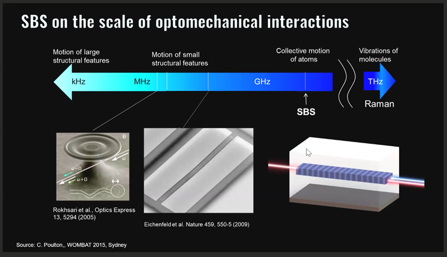
Therefore, Prof. David Marpaung with the Nanophotonics Research Group at the University of Twente carried out development and research on stimulated Brillouin scattering (SBS). “SBS can be applied on many devices, from a variety of sensors, amplifiers, gyroscope, RF light processors, quantum memory, and lasers with high spectral purity,” explained Prof. David.
One way to optimize the SBS function is by separating the two layers of silicon nitride. “Through optimizing the separation between two layers of the silicon nitride, we open a gigahertz acoustic waveguide in this platform for the first time and produced an SBS coefficient value up to 15 times higher than previously possible in a silicon nitride waveguide,” described Prof. David.
Certainly, the effort to mobilize SBS in photonic silicon gives rise to pros and cons. On one hand, this effort resulted in various advantages such as production cost efficiency, as silicon can be produced en masse, and it is also compatible with CMOS. Moreover, silicon possesses a high index and small mode area. Its radiation pressure was also amplified to the nanoscale. However, on the other, silicon has a relatively high propagation and nonlinear loss, as well as experiences acoustic leaks.
To further elaborate, research regarding scattered Brillouin scattering (SBS) will be continued with the development of the SBS integrated circuit, which could be applied to various devices such as acoustic-based sensors, MWP signal processors, non-reciprocity and isolators, laser and frequency combs, dynamic grating, pulse shaping, and tunable delay and memory.
Reporter: Yoel Enrico Meiliano (Food Engineereing, 2020)
Translator: Firzana Aisya (Bioengineering, 2021)

.jpg)
.jpg)


.jpg)
